Diode
We all are familiar with the technical hub of the world that is the SILICON VALLEY . The name Silicon has come after the rise of Semiconductors in the field of electronics especially Silicon Today, most semiconductor chips and transistors are created with silicon.Silicon is also called as heart of electronics.
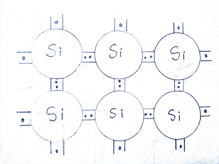
A diode is the simplest possible semiconductor device. It is generally made up of Silicon i.e. Extrinsic type of silicon meaning doped with impurities giving rise to n-type and p-type semiconductors
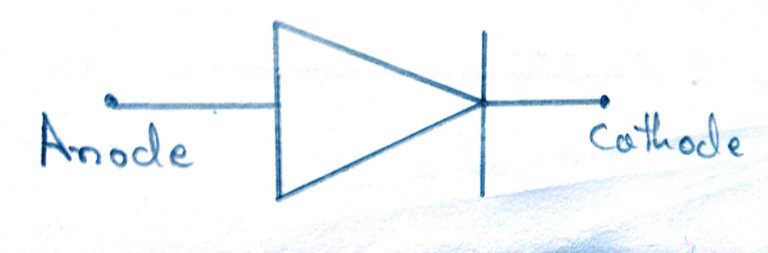
N-type and P-type silicon are not that amazing by themselves; but when you put them together, you get some very interesting behavior at the junction. That’s what happens in a diode.
A diode allows current to flow in one direction but not the other. You may have seen one way roads which allows traffic vehicles only in one direction .Similarly a diode is a one-way road which allows the flow of electrons only in a given direction
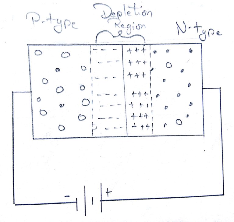
When you put N-type and P-type silicon together as shown in this diagram, you get a very interesting phenomenon that gives a diode its unique properties.
Even though N-type silicon by itself is a conductor, and P-type silicon by itself is also a conductor, the combination shown in the diagram does not conduct any electricity. The negative electrons in the N-type silicon get attracted to the positive terminal of the battery. The positive holes in the P-type silicon get attracted to the negative terminal of the battery. No current flows across the junction because the holes and the electrons are each moving in the wrong direction.This Results in broadening of the depletion region .In this no current flows even though very high voltage is applied.But there is a limit in the applied voltage , If the voltage is increased even after the reverse breakdown voltage of the diode , then it results in Avalanche Breakdown which permanently damages the diode . This characteristics of Diode are seen when connected in Reverse bias
When reverse-biased, an ideal diode would block all current but real diode let’s perhaps 10 microamps through — not a lot, but still not perfect.
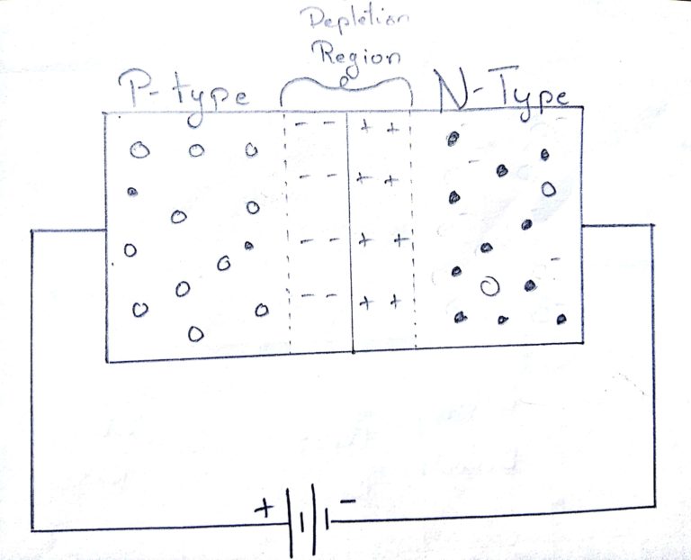
If we flip the battery around, that is if we connect the diode in the forward direction than it conducts electricity normally. The free electrons in the N-type silicon are repelled by the negative terminal of the battery. The holes in the P-type silicon are repelled by the positive terminal. At the junction between the N-type and P-type silicon, holes and free electrons meet which results in a narrower depletion region . The holes and free electrons cease to exist, and new holes and electrons spring up to take their place. The effect is that current flows through the junction.When forward-biased, there is a small amount of voltage necessary to get the diode going. In silicon, this voltage is about 0.7 volts. This voltage is needed to start the hole-electron combination process at the junction.
Thus we can say that a device that blocks current in one direction while letting current flow in another direction is called a diode. Diodes can be used in a number of ways. For example, a device that uses batteries often contains a diode that protects the device if you insert the batteries backward. The diode simply blocks any current from leaving the battery if it is reversed — this protects the sensitive electronics in the device.
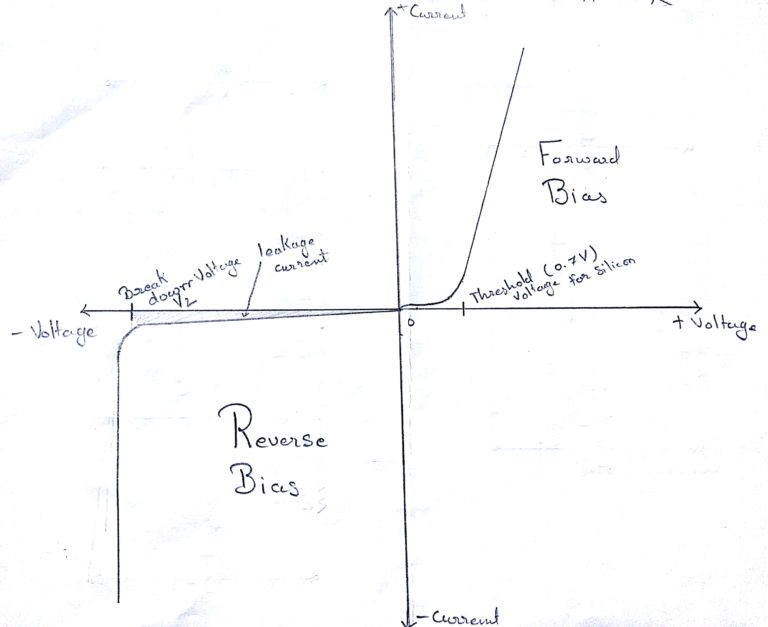
The figure above shows the characteristics of Diode in Forward and Reverse Bias.
Half Wave Rectifier :
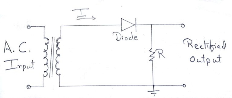
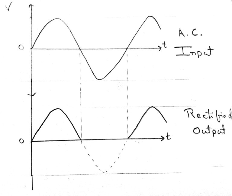
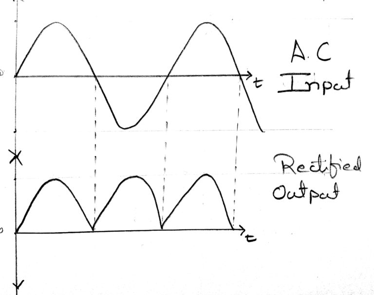
The figure shown is the diagram of Half Wave Rectifier. Main function of the rectifier is to convert the AC signal to DC signal. As the name suggests the Half wave rectifier it utilizes only the positive half cycle of the AC signal while the negative half cycle is not utilized.
In half wave rectifier, when positive cycle is there at the Anode , it makes the diode in the forward bias and will allow the current to flow for that period of time .
When negative cycle comes, the potential at the anode of the diode becomes negative with respect to cathode and thus the diode becomes reverse bias and blocks the flow of current through it.
The AC power source only supplies power to the load one half every full cycle, meaning that half of its capacity is unused. Half-wave rectification is, however, a very simple way to reduce power to a resistive load.
For most power applications, half-wave rectification is insufficient for the task. The harmonic content of the rectifier’s output waveform is very large and consequently difficult to filter.
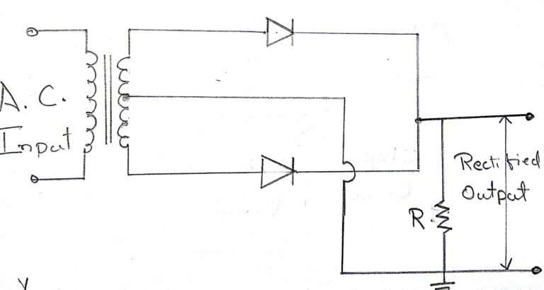
Full Wave Rectifier :
If we need to rectify AC power to obtain the full use of both half-cycles of the sine wave, a different rectifier circuit configuration must be used. Such a circuit is called a full-wave rectifier. One kind of full-wave rectifier, is the center-tap design, which uses a transformer with a center-tapped secondary winding and two diodes,
This circuit’s operation is easily understood one half-cycle at a time. Consider the first half-cycle, when the source voltage polarity is positive (+) on top and negative (-) on bottom. At this time, only the top diode is conducting; the bottom diode is blocking current, and the load “sees” the first half of the sine wave, positive on top and negative on bottom. Only the top half of the transformer’s secondary winding carries current during this half-cycle
During the next half-cycle, the AC polarity reverses. Now, the other diode and the other half of the transformer’s secondary winding carry current while the portions of the circuit formerly carrying current during the last half-cycle sit idle. The load still “sees” half of a sine wave, of the same polarity as before: positive on top and negative on bottom.
One disadvantage of this full-wave rectifier design is the necessity of a transformer with a center-tapped secondary winding. If the circuit is one of high power, the size and expense of a suitable transformer is significant. Consequently, the center-tap rectifier design is only seen in low-power applications.
So a more popular full-wave rectifier design exists, and it is built around a four-diode bridge configuration. For obvious reasons, this design is called a full-wave bridge.
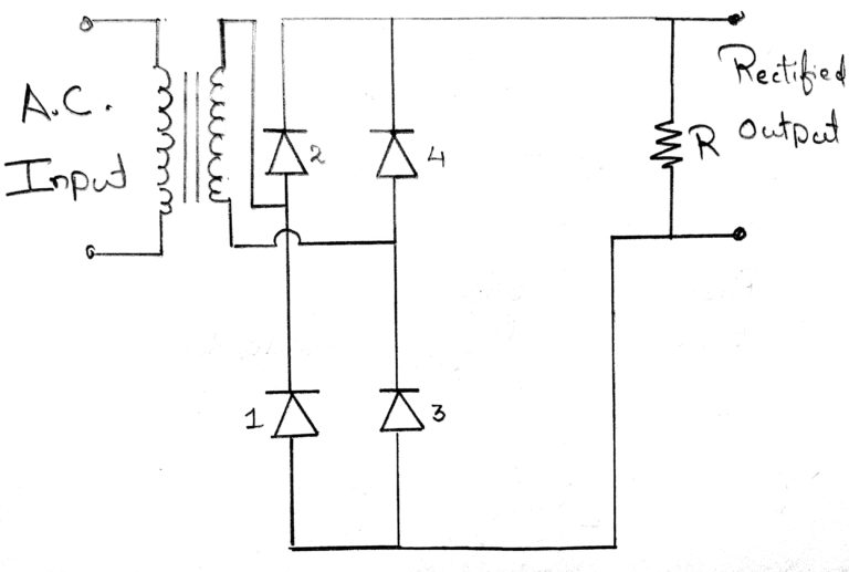
In this configuration during the positive cycle the positive voltage flows through diode 2 where as the negative potential flows through diode 3 . Similarly in the negative cycle dode 4 will conduct positive voltage whereas diode 1 will conduct negative voltage.
The current flow is through two diodes in series for both polarities. Thus, two diode drops of the source voltage are lost (0.7·2=1.4 V for Si) in the diodes. This is a disadvantage compared with a full-wave center-tap design. This disadvantage is only a problem in very low voltage power supplies.