FET Basics
The name itself suggests the meaning i.e. field-effect transistor (FET) is a transistor that uses an electric field to control the electrical behavior of the device. Many different implementations of field effect transistors exist. Field effect transistors generally display very high input impedance at low frequencies.
The FET consists of a semiconductor channel with electrodes at either end referred to as the drain and the source.
A control electrode called the gate is placed in very close proximity to the channel so that its electric charge is able to affect the channel.
By controlling the size and shape of the conductive channel. the gate of the FET controls the flow of carriers (electrons or holes) flowing from the source to drain.
The semiconductor channel where the current flow occurs may be either P-type or N-type. This gives rise to two types or categories of FET known as P-Channel and N-Channel FETs.
As it is only the electric field that controls the current flowing in the channel, the device is said to be voltage operated and it has a high input impedance, usually many megaohms. This can be a distinct advantage over the bipolar transistor that is current operated and has a much lower input impedance.
The electric field to control the current is applied to a third electrode known as a gate.
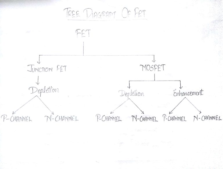
The external field on the gate may serve to deplete the channel of carriers, in which case the FET is known as a depletion mode FET, or it may serve to enhance the carriers in the channel when it is known as an enhancement mode FET.
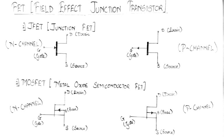
There are various types of FET: but the two main types are JFET and MOSFET
Tree diagram of FET types
There are many different types of FET on the market for which there are various names. Some of the major categories are :
Junction FET, JFET : This form of FET uses a reverse biased diode junction to provide the isolation from the channel. It is the most basic type of FET, and the one that was first developed. However it still provides excellent service in many areas of electronics.
Insulated Gate FET / Metal Oxide Silicon FET MOSFET : This type of FET uses an insulated later between the gate and the channel. Typically this is formed from a layer of oxide of the semiconductor. The most common type of IGFET. The MOSFET – Metal Oxide Silicon FET. Here the gate is made of a layer of metal set down on the silicon oxide which in turn is on the silicon channel.
VMOS : VMOS standard for vertical MOS. It is a type of FET that uses a vertical current flow to improve the switching and current carrying performance. VMOS FETs are widely used for power applications.
There are few other types like:
Dual Gate MOSFET
MESFET
HEMT / PHEMT
FinFET
Main FET specifications
The datasheet includes some of the FET specifications. Some are important for JFET while some for MOSFET and others:
Drain-Source Voltage, VDSS : This is a rating for the maximum drain-source voltage that can be applied without causing avalanche breakdown. The parameter is normally stated for the case where the gate is shorted to the source and for a temperature of 25°C. Depending on temperature, the avalanche breakdown voltage could actually be less than the VDSS rating.
Gate source voltage, VGS : The FET parameter VGS is the rating for the maximum voltage that can be tolerated between the gate and source terminals. The purpose for including this parameter in the data sheet is to prevent damage of the gate oxide.
Threshold voltage VGS(TH) : The threshold voltage VGS(TH) is the minimum gate voltage that can form a conducting channel between the source and the drain. It is normally quoted for a given source drain current.
Gate source cut-off voltage , VGS(off) : The gate source cut-off voltage is really a turn-off specification. It defines the threshold voltage for a given residual current, so the device is basically off but on the verge of turning on.
Drain current at zero gate voltage , Idss : This FET parameter is the maximum continuous current the device can carry with the device fully on. Normally it is specified for a particular temperature, typically 25°C. The actual switching current should be limited to less than half of the Idss at TC = 25°C rating in a hard switched application.
Input capacitance, Ciss : The input capacitance parameter for a FET is the capacitance that is measured between the gate and source terminals with the drain shorted to the source for AC signals. In other words this is effectively the capacitance between the gate and channel. This can be expressed as:
Drain-source on resistance, Rds(on) : With the FET turned hard on, this is the resistance in ohms exhibited across the channel between the drain and source. It is particularly important in switching applications from logic to power switching as well as in RF switching, including applications in mixers.
Power dissipation, Ptot : This FET specification is the maximum continuous power the device can dissipate. It is normally specified in free standing in air, or with the base held at a given temperature, typically 25°C.
Why FET when you have BJT?
FET [Field Effect Transistor] |
BJT [Bipolar Junction Transistor] |
|---|---|
| High Current gain | Low current gain |
| Low Voltage gain | High voltage gain |
| High output impedance | Low output impedance |
| Very High input impedance | Low input impedance |
| Low Noise generation | Medium Noise Generation |
| Fast switching time | Medium switching time |
| Difficult to Bias | Easy to bias |
| Some need an input to turn it "OFF" | Requires zero input to turn it "OFF" |
| It is a Voltage controlled device | It is a Current controlled device |
| More expensive than BJT | Cheaper than FET |
| It can be Easily damaged | It is Robust |