Transistor Configurations
Common Base (CB) Configuration : no current gain but voltage gain
Common Collector (CC) Configuration : current gain but no voltage gain
Common Emitter (CE) Configuration : current gain and voltage gain
The Common Base (CB) Configuration
As the name suggests, in the Common Base or grounded base configuration, the BASE connection is common to both the input signal AND the output signal (i.e. to the emitter end as well as the collector end). Here, the question is where shall the input be applied and the output be taken from.
The input signal is applied between the transistors base and the emitter terminals, while the corresponding output signal is taken from between the base and the collector terminals. The base terminal is usually grounded (GND) or can be connected to some fixed reference voltage point.
The input current which is flowing into the emitter terminal is quite large as its the sum of both the base current and collector current respectively. Therefore, the emitter current input is more than the collector current output resulting in a current gain of “1” (unity) or less, for this type of circuit. In other words the common base configuration “attenuates” the input signal.
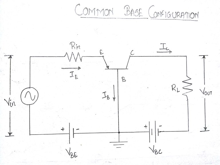
The Common Base Transistor Circuit
This circuit is not commonly used due to its unusually high voltage gain characteristics. Its input characteristics represent that of a forward biased diode while the output characteristics represent that of an illuminated Photo-Diode.
Common Base Configuration also has a high ratio of output to input resistance or better say, “load” resistance ( RL ) to “input” resistance ( Rin ) giving it a value of “Resistance Gain”. Then the voltage gain ( Av ) for a common base configuration is therefore given as:
Common Base Voltage Gain
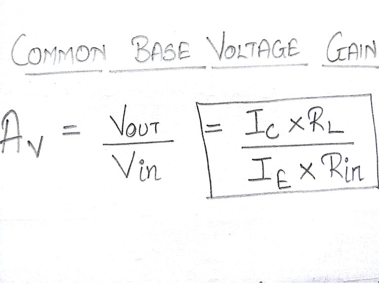
Where: Ic/Ie is the current gain, alpha ( α ) and RL/Rin is the resistance gain.
The common base circuit is generally used in single stage amplifier circuits such as microphone pre-amplifier or radio frequency ( Rƒ ) amplifiers due to its very good high frequency response.
The Common Emitter (CE) Configuration
In the Common Emitter or grounded emitter configuration, the input signal is applied between the base and the emitter, while the output is taken from between the collector and the emitter. I.e. The emitter is common between the base and the collector.
This type of configuration is the most commonly used circuit. Transistors when made as amplifiers this configuration is the best. It represents the “normal” method of bipolar transistor connection. So while understanding Transistors in general usually the construction or circuit diagram of Common Emitter Type Configuration is used.
This configuration produces the highest current and power gain of all the three bipolar transistor configurations. This is mainly because the input impedance is LOW as it is connected to a forward biased PN-junction, while the output impedance is HIGH as it is taken from a reverse biased PN-junction.
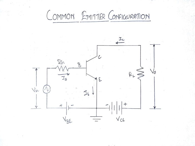
The Common Emitter Amplifier Circuit
In this type of configuration, the current flowing out of the transistor must be equal to the currents flowing into the transistor as the emitter current is given as Ie = Ic + Ib.
Any small change in the base current ( Ib ), will result in a much larger change in the collector current ( Ic ).
As the load resistance ( RL ) is connected in series with the collector, the current gain of the common emitter transistor configuration is quite large as it is the ratio of Ic/Ib. A transistors current gain is given the Greek symbol of Beta, ( β ).
Then, small changes in current flowing in the base will thus control the current in the emitter-collector circuit. Typically, Beta has a value between 20 and 200 for most general purpose transistors. So if a transistor has a Beta value of say 100, then one electron will flow from the base terminal for every 100 electrons flowing between the emitter-collector terminal.
Common Emitter Current Gain:
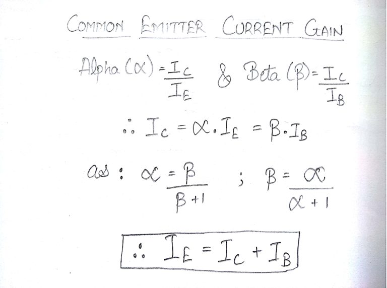
The current gain of the transistor can be given as:
Where: “Ic” is the current flowing into the collector terminal, “Ib” is the current flowing into the base terminal and “Ie” is the current flowing out of the emitter terminal.
The Common Collector (CC) Configuration
In the Common Collector or grounded collector configuration, the collector is now common through the supply. The input signal is connected directly to the base, while the output is taken from the emitter load. This type of configuration is commonly known as a Voltage Follower or Emitter Follower circuit.
The common collector, or emitter follower configuration is very useful for impedance matching applications because of the very high input impedance, in the region of hundreds of thousands of Ohms while having a relatively low output impedance.
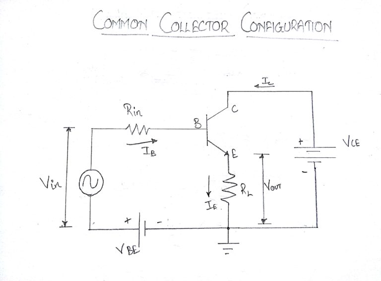
The Common Collector Transistor Circuit
In the common collector configuration the load resistance is situated in series with the emitter so its current is equal to that of the emitter current.
As the emitter current is the combination of the collector AND the base current combined, the load resistance in this type of transistor configuration also has both the collector current and the input current of the base flowing through it. Then the current gain of the circuit is given as:
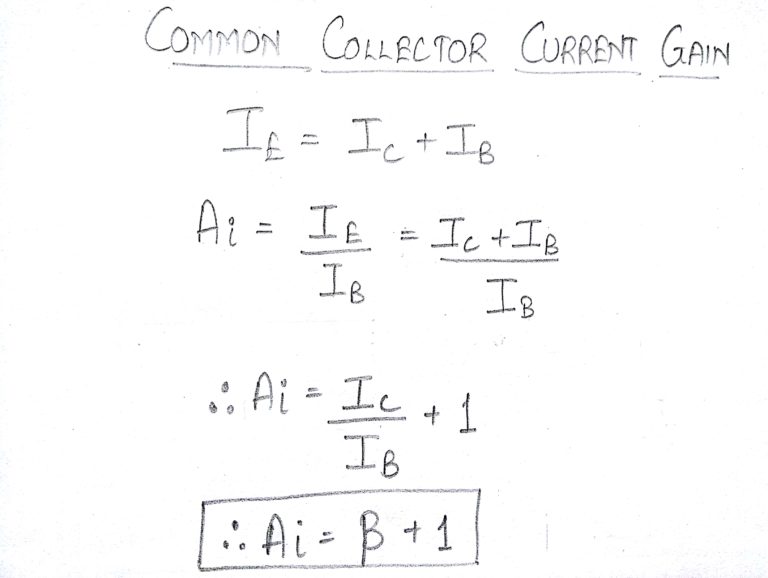
This configuration is a non-inverting circuit in that the signal voltages of Vin and Vout are “in-phase”. It has a voltage gain that is always less than “1” (unity). The load resistance of the common collector transistor receives both the base and collector currents giving a large current gain (as with the common emitter configuration) therefore, providing good current amplification with very little voltage gain.