SR-F/F and D-F/F
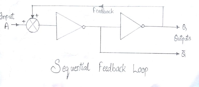
Sequential Feedback Loop
The two inverters or NOT gates are connected in series with the output at Q fed back to the input. Unfortunately, this configuration never changes state because the output will always be the same, either a “1” or a “0”, it is permanently set. However, we can see how feedback works by examining the most basic sequential logic components, called the SR flip-flop.
Flip Flop
Flip flop is a sequential circuit which generally samples its inputs and changes its outputs only at particular instants of time and not continuously. Flip flop is said to be edge sensitive or edge triggered rather than being level triggered like latches.
S-R Flip Flop
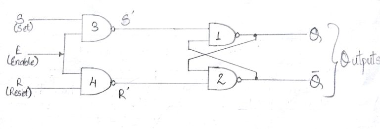
It is basically S-R latch using NAND gates with an additional enable input. It is also called as level triggered SR-FF. For this, circuit in output will take place if and only if the enable input (E) is made active. In short this circuit will operate as an S-R latch if E = 1 but there is no change in the output if E = 0.
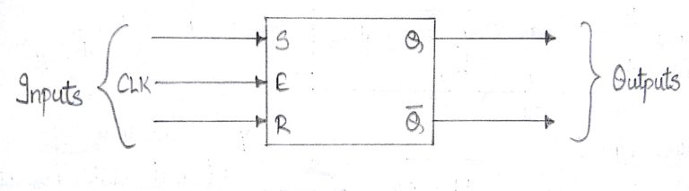
Block Diagram :
Circuit Diagram :
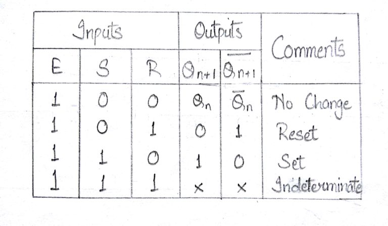
Truth Table :
Operation
| S.N. | Condition | Operation |
|---|---|---|
| 1 | S = R = 0 : No change | If S = R = 0 then output of NAND gates 3 and 4 are forced to become 1. Hence R’ and S’ both will be equal to 1. Since S’ and R’ are the input of the basic S-R latch using NAND gates, there will be no change in the state of outputs. |
| 2 | S = 0, R = 1, E = 1 | Since S = 0, output of NAND-3 i.e. S’ = 1 and E = 1 the output of NAND-4 i.e. R’ = 0. Hence Qn+1 = 0 and Qn+1 bar = 1. This is reset condition. |
| 3 | S = 1, R = 0, E = 1 | Output of NAND-3 i.e. S’ = 0 and output of NAND-4 i.e. R’ = 1. Hence output of S-R NAND latch is Qn+1 = 1 and Qn+1 bar = 0. This is the reset condition. |
| 4 | S = 1, R = 1, E = 1 | As S = 1, R = 1 and E = 1, the output of NAND gates 3 and 4 both are 0 i.e. S’ = R’ = 0. Hence the Race condition will occur in the basic NAND latch. |
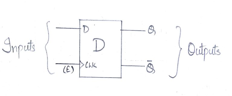
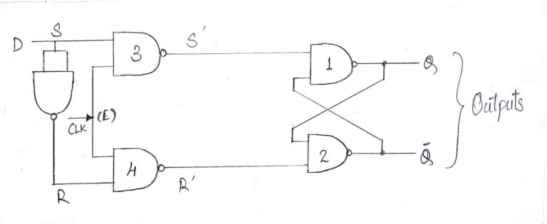
Delay Flip Flop / D Flip Flop
Delay Flip Flop or D Flip Flop is the simple gated S-R latch with a NAND inverter connected between S and R inputs. It has only one input. The input data is appearing at the output after some time. Due to this data delay between i/p and o/p, it is called delay flip flop. S and R will be the complements of each other due to NAND inverter. Hence S = R = 0 or S = R = 1, these input condition will never appear. This problem is avoid by SR = 00 and SR = 1 conditions.
Block Diagram :
Circuit Diagram :
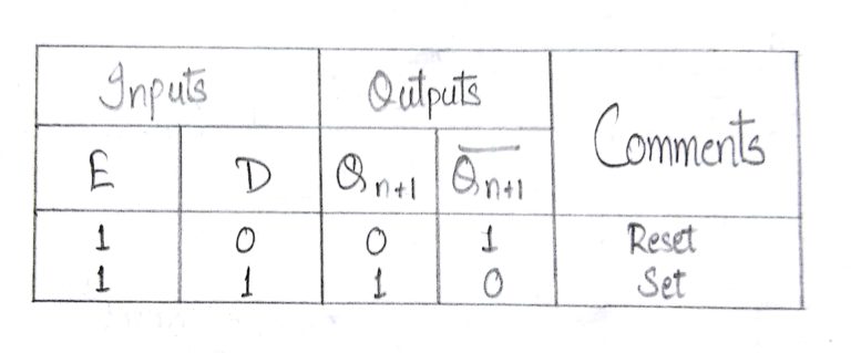
Truth Table :
Operation
| S.N. | Condition | Operation |
|---|---|---|
| 1 | E = 0 | Latch is disabled. Hence no change in output. |
| 2 | E = 1 and D = 0 | If E = 1 and D = 0 then S = 0 and R = 1. Hence irrespective of the present state, the next state is Qn+1 = 0 and Qn+1 bar = 1. This is the reset condition. |
| 3 | E = 1 and D = 1 | If E = 1 and D = 1, then S = 1 and R = 0. This will set the latch and Qn+1 = 1 and Qn+1 bar = 0 irrespective of the present state. |