JFET – MOSFET
The junction gate field-effect transistor (JFET or JUGFET) is the simplest type of field-effect transistor. They are three-terminal semiconductor devices that can be used as electronically-controlled switches, amplifiers, or voltage-controlled resistors.
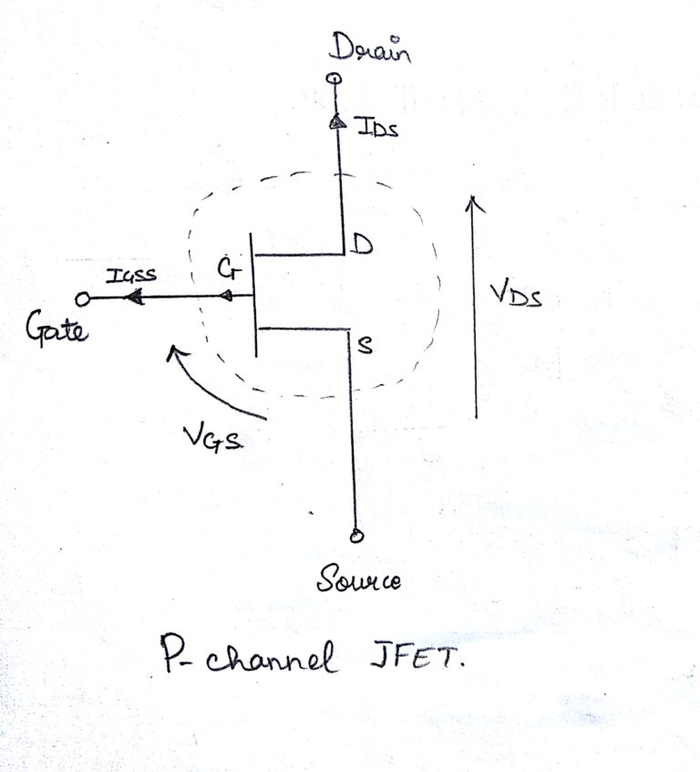
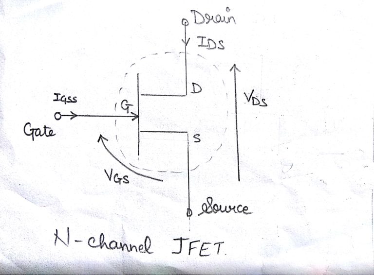
Junction field effect transistor or JFET consists of a section of silicon whose conductance is controlled by an electric field. The section of silicon through which the current flows is called the channel, and it consists of, either N-type or P-type silicon.
The FET however, uses the voltage that is applied to their input terminal, called the Gate to control the current flowing through them resulting in the output current being proportional to the input voltage. As their operation relies on an electric field (hence the name field effect) generated by the input Gate voltage, this then makes the Field Effect Transistor a “VOLTAGE” operated device.
The connections at either end of the device are known as the source and drain. The electric field to control the current is applied to a third electrode known as a gate.
JFET OPERATION
In FET voltages appearing on the gate, control the operation of the device, making it a voltage controlled device.
Both N-channel and P-channel devices operate in similar ways, although the charge carriers are inverted, i.e. electrons in one and holes in the other.
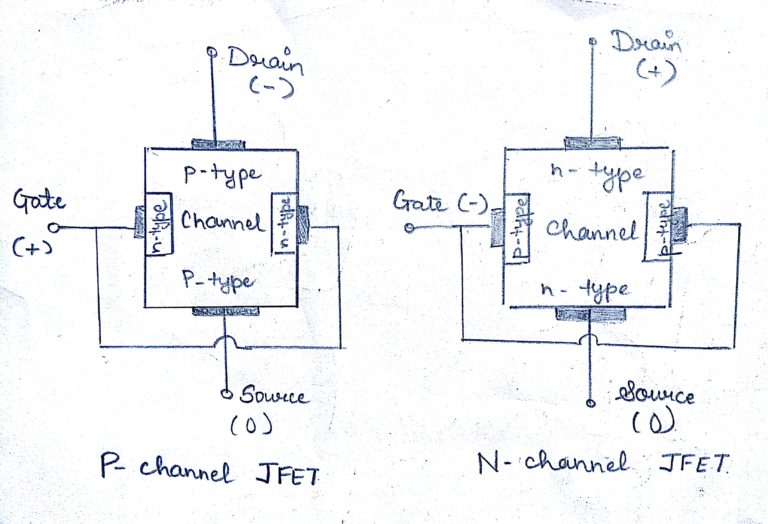
N-Channel is always preferred as it has electrons as majority carriers which in turn results in more current.
The thickness of this layer varies in accordance with the magnitude of the reverse bias on the junction. In other words when there is a small reverse bias the depletion layer only extends a small way into the channel and there is a large area to conduct current. When a large negative bias is placed on the gate, the depletion layer increases, extending further into the channel, reducing there area over which current can be conducted. With increasing bias the depletion layer will eventually increase to the degree that it extends right across the channel, and the channel is said to be cut off.
Assuming an n-type channel, When a current flows in the channel the situation becomes slightly different. With no gate voltage electrons in the channel will be attracted by the positive potential on the drain, and will flow towards it enabling a current to flow within the device, and hence within the external circuit. The magnitude of the current is dependent upon a number of factors and included the cross sectional area of the channel, its length and conductivity (i.e. the number of free electrons in the material) and the voltage applied.
From this it can be seen that the channel acts as a resistor, and there will be a voltage drop along its length. As a result of this it means that the p-n junction becomes progressively more reverse biased as the drain is approached. Consequently the depletion layer becomes thicker nearer the drain. As the reverse bias on the gate is increased a point is reached where the channel is almost closed off by the depletion layer. However the channel never completely closes. The reason for this is that the electrostatic forces between the electrons cause them to spread out, giving a counter effect to the increase in thickness of the depletion layer. After a certain point the field around the electrons flowing in the channel successfully opposes any further increase in the depletion layer. The voltage at which the depletion layer reaches its maximum is called the pinch off voltage.
Applications for JFETs :
JFETs can be used for several applications including:
High Input Impedance Amplifier
Low-Noise Amplifier
Differential Amplifier
Constant Current Source
Analog Switch or Gate
Voltage Controlled Resistor
MOSFET
The MOSFET has a number of different characteristics compared to the junction FET, and as a result it can be used in a number of different areas and it is able to provide excellent performance.
MOSFETs provide many advantages. In particular they offer a very high input impedance and they are able to be used in very low current circuits. This is particularly important for integrated circuit technology where power limitations are a major consideration.
One particular area where MOSFET technology is used is within CMOS logic integrated circuits. The extraordinarily high input impedance means that these circuits are able to consume very low power levels and this means that high levels of integration can be achieved.
MOSFET symbol
There a several MOSFET circuit symbols that are used. Some MOSFET symbols are equivalents of each other, while others indicate more detail about the MOSFET itself.
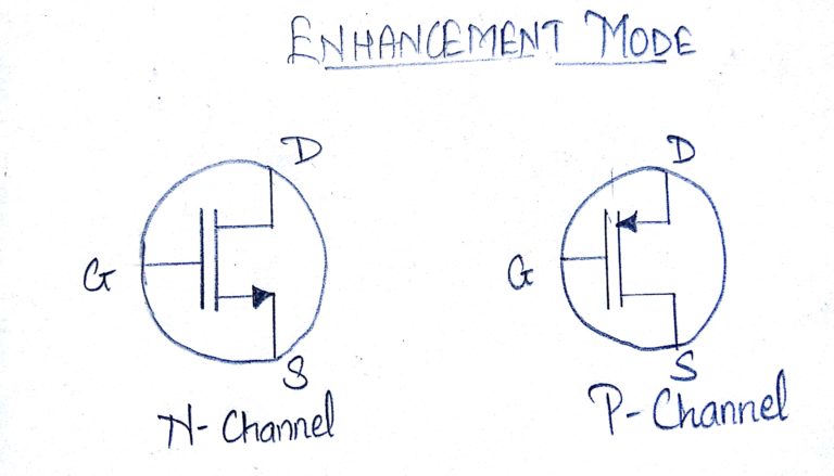
As there are several varieties of MOSFET, the symbols used to indicate them need to be different.
MOSFET symbol used above generally indicates that the device has a bulk substrate – this is indicated by the arrow on the central area of the substrate.
The MOSFET provides some key features for circuit designers in terms of their overall performance.
Gate construction: Gate is physically insulated from the channel by an oxide layer. Voltages applied to the gate control the conductivity of the channel as a result of the electric field induced capacitively across the insulating dielectric layer.
N / P channel: Both N-channel and P-channel variants are available
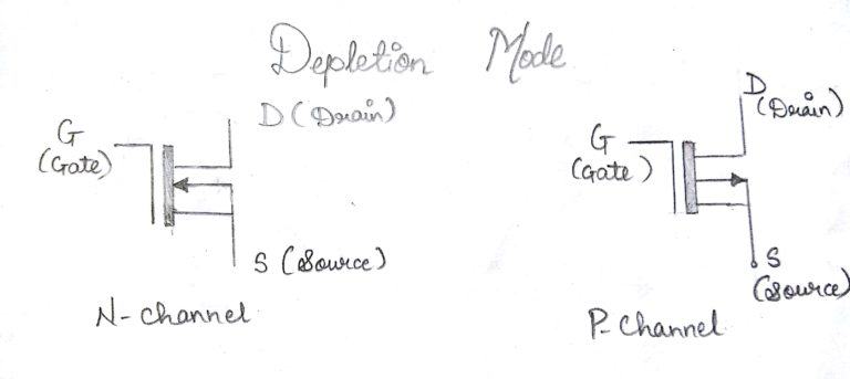
Enhancement / depletion: Both enhancement and depletion types are available. As the name suggests the depletion mode MOSFET acts by depleting or removing the current carriers from the channel, whereas the enhancement type increases the number of carriers according to the gate voltage.
The two main types of MOSFET are N-channel and P-channel. Each has different features:
| COMPARISON OF THE KEY FEATURES OF N-CHANNEL AND P-CHANNEL MOSFETS | ||
|---|---|---|
| PARAMETER | N-CHANNEL | P-CHANNEL |
| Source / drain material | N-Type | P-Type |
| Channel material | P-Type | N-Type |
| Threshold voltage Vth | negative | doping dependent |
| Substrate material | P-Type | P-Type |
| Inversion layer carriers | Electrons | Holes |
Like other forms of FET, the current flowing in the channel of the MOSFET is controlled by the voltage present on the gate. As such MOSFETs are widely used in applications such as switches and also amplifiers. They are also able to consume very low levels of current and as a result they are widely used in microprocessors, logic integrated circuits and the like.
Also like other forms of FET, the MOSFET is available in depletion mode and enhancement mode variants. The enhancement mode is what may be termed normally OFF, i..e when the VGS gate source voltage is zero and requires a gate voltage to turn it on, whereas the other form, depletion mode devices are normally ON when VGS is zero.
There are basically three regions in which MOSFETs can operate:
Cut-off region : In this region of the MOSFET is in a non-conducting state, i.e. turned OFF – channel current IDS = 0. The gate voltage VGS is less than the threshold voltage required for conduction.
Linear region : In this linear region the channel is conducting and controlled by the gate voltage. For the MOSFET to be in this state the VGS must be greater than the threshold voltage and also the voltage across the channel, VDS must be greater than VGS.
Saturation region : In this region the MOSFET is turned hard on. The voltage drop for a MOSFET is typically lower than that of a bipolar transistor and as a result power MOSFETs are widely used for switching large currents.